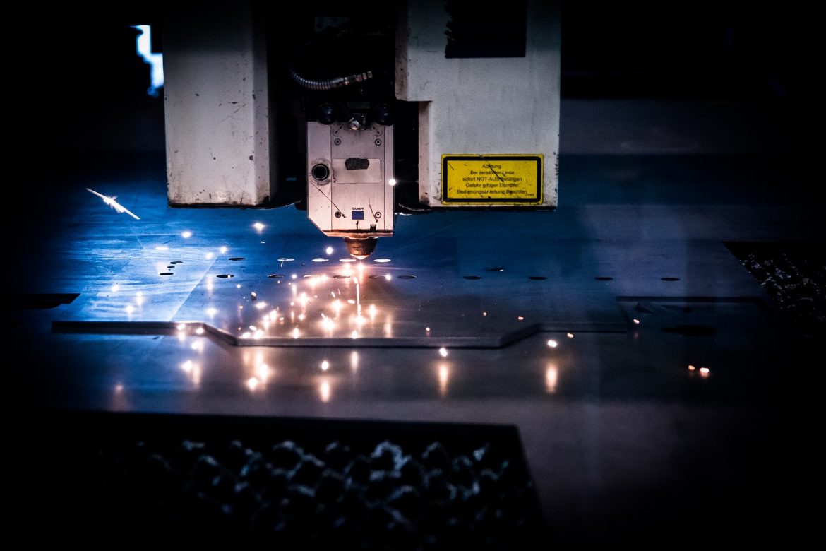
A laser marking process is crucial for the manufacture of silicon wafers. In an optical laser machine a concentrated beam of light is used to mark semiconductor packages permanently.
Laser is more than just a word. It stands for “Light Amplification by Stimulated Emission of Radiation.” The device generates specialized light particles targeted at precise locations by stimulating an atom. With the aid of a marking laser, this can be done with accuracy.
It is possible to track wafers throughout the manufacturing process with laser marking. This requires an automatic reading of the laser markings. Additionally, the marking must not adversely affect the underlying processes, and the wafer must not be damaged as a result. Keeping it perfect is essential. For more information, visit lasitlaser.de.
We offer silicon wafer laser marking services as part of our overall process.
What is the process of making a silicon wafer?
Laser marking is what it sounds like. Wafers are marked with lasers to identify them. As with semiconductors, wafers can be found in almost every type of electronic device. They have a flat surface, a circular shape, and are mirrored in appearance.
Due to the absence of impurities in silicon wafers, laser marking must be performed with extreme care to ensure they remain faultless.
Laser-enhanced annexes
By using a laser beam, surfaces can be heated extremely efficiently during annealing. Heat (oxidation) causes oxygen to diffuse below the surface. Once everything has cooled, you can see a change in color.
The color of annealed products can range from yellow to red to green. This color can change depending on the temperature during marking. There are three variables that determine whether the temperature increases or decreases:
- Intensity of the pulse
- Speed of light
- Each line is followed by a pass
With these lasers, characters can be rendered as small as millimeters tall. Due to its excellent results, lasers are used to mark silicon-based wafers during an annealing process.
The Basics of Laser Marking
Marking silicon wafers requires the use of computers. At this point in the process, the marking document shows a map of the wafer. It contains information about the parameters, functions, and so on. There is a preview view of how the data will be translated into silicon on the other side of the screen.
When the laser marking machine is set up properly, the wafer is placed inside. Mechanical hand is used to pick up the wafer and bring it to the marking station. Automated processes require no human interaction at any point, as the entire process is automated.
Read More: Optical Thin Film
After the machine has found its target location, a laser is directed at the wafer surface. In the end, the project will be delivered to the receiving box so that it can be removed.
The advantages of laser marking are numerous
Precision-Oriented
Laser marking is a great choice for manufacturing wafers due to its precision. Its superior technology ensures that even the tiniest details are captured perfectly and accurately. As small as a millimeter, silicon wafer markings can be read by computers for easy tracking.
Speedy
Laser marking is fast and precise, as well as being extremely precise. It only takes minutes to mark entire silicon wafer stacks, from placement to marking to completion. While laser annealing is slower, it leaves a superb finish without leaving any residue behind.
Surface-only application
Laser marking does not actually remove material from silicon wafer surfaces. It only changes the color of the material underneath the surface. All conditions remain the same.